
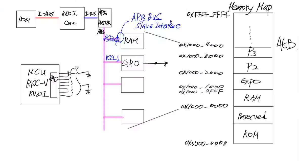
APB Slave Interface RAM Design
< Design Specification >
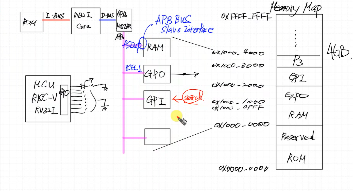
- Address 기준으로 broadcast 하는 구조 : BUS 구조
/* APB_Slave 구조 참고 */
if (PWRITE) begin // 쓰기 동작
    case (PADDR[3:2]) // 주소에 따른
        2'd0: slv_reg0 <= PWDATA;
        2'd1: slv_reg1 <= PWDATA;
        2'd2: slv_reg2 <= PWDATA;
        2'd3: slv_reg3 <= PWDATA;
    endcase
end else begin // 읽기 동작
    case (PADDR[3:2]) // 주소에 따른
        2'd0: PRDATA <= slv_reg0;
        2'd1: PRDATA <= slv_reg1;
        2'd2: PRDATA <= slv_reg2;
        2'd3: PRDATA <= slv_reg3;
    endcase
end
< Simulation >
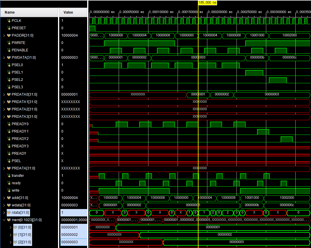
- APB는 CPU 는 ready 신호가 들어올 때까지 몇 클럭이든 대기
- AHB는 파이프라인구조라서 대기하는 시간이 짧음
- RAM 스택포인터 위치 0x1000_0000 ~ 0x1000_0FFF 맞춰서 SP를 RAM 최상단으로 초기화해야 함
< SW 검증 : Store, Load Test>
int main()
{
    int a, b, c;

    a = 1;
    b = 2;
    c = a + b;

    return 0;
}
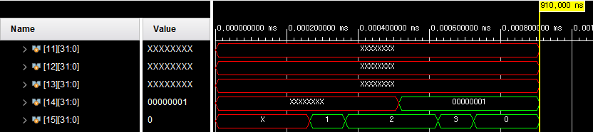
< Simulation >
GPO Design
< Design Specification >
- GPO 를 만들어서 연결을 원하며, LED도 연결한다.
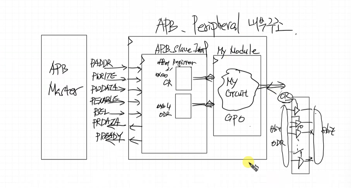
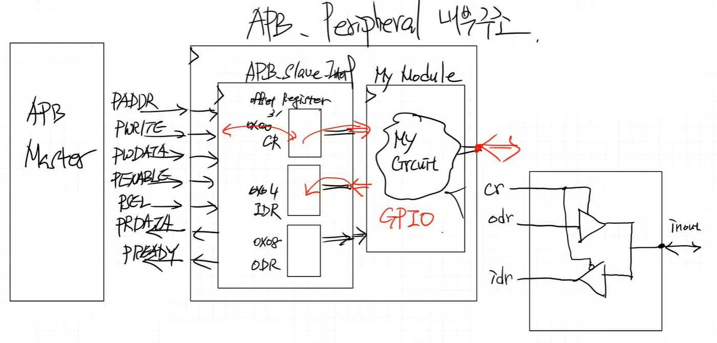
< APB_Peripheral 내부 구조 >
< SW 검증 : GPO 동작 >
#include <stdint.h>

#define APB_BASE    0x10000000
#define GPO_BASE    (APB_BASE + 0x1000)
#define GPO_CR      *(uint32_t *)(GPO_BASE + 0x00)
#define GPO_ODR     *(uint32_t *)(GPO_BASE + 0x04)

int main()
{
    uint32_t data = 0;

    GPO_CR = 0xff;
    while(1)
    {
        GPO_ODR = data;
        data = GPO_ODR;
        data = data ^ 1;
    }
    return 0;
}
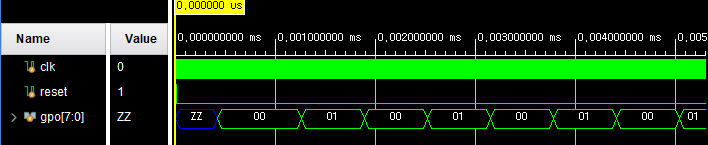
< Simulation >
< SW 검증 : LED Shift Test >
#include <stdint.h>

#define APB_BASE    0x10000000
#define GPO_BASE    (APB_BASE + 0x1000)
#define GPO_CR      *(uint32_t *)(GPO_BASE + 0x00)
#define GPO_ODR     *(uint32_t *)(GPO_BASE + 0x04)

void delay(uint32_t t);

int main()
{
    uint32_t data = 1;

    GPO_CR = 0xff;
    while(1)
    {
        GPO_ODR = data;
        delay(1000);
        data = (data >> 7) | (data << 1);
    }
    return 0;
}

void delay(uint32_t t)
{
    for (uint32_t i=0; i<t; i++) {
        for (uint32_t j=0; j<1000; j++);
    }
}
GPI Design
< SW 검증 : LED Switching Test >
#include <stdint.h>

#define APB_BASE    0x10000000
#define GPO_BASE    (APB_BASE + 0x1000)
#define GPO_CR      *(uint32_t *)(GPO_BASE + 0x00)
#define GPO_ODR     *(uint32_t *)(GPO_BASE + 0x04)
#define GPI_BASE    (APB_BASE + 0x2000)
#define GPI_CR      *(uint32_t *)(GPI_BASE + 0x00)
#define GPI_IDR     *(uint32_t *)(GPI_BASE + 0x04)

//void delay(uint32_t t);

int main()
{
    uint32_t data = 0;

    GPO_CR = 0xff;
    GPI_CR = 0xff;
    while(1)
    {
        data = GPI_IDR;
        GPO_ODR = data;
        //delay(1000);
        //data = (data >> 7) | (data << 1);
    }
    return 0;
}
/*
void delay(uint32_t t)
{
    for (uint32_t i=0; i<t; i++) {
        for (uint32_t j=0; j<1000; j++);
    }
}
*/
GPIO Design
< 파일 >
sources (Class)
simulation (Class)
constrs (Class)
HW : FND_Peripheral Design
< SW 검증 : FND 0~9999 Counter 동작 >
#include<stdint.h>
#define APB_BASE    0x10000000
#define GPO_BASE    (APB_BASE + 0x1000)
#define GPO_CR      *(uint32_t *)(GPO_BASE + 0x00)
#define GPO_ODR     *(uint32_t *)(GPO_BASE + 0x04)
#define GPI_BASE    (APB_BASE + 0x2000)
#define GPI_CR      *(uint32_t *)(GPI_BASE + 0x00)
#define GPI_IDR     *(uint32_t *)(GPI_BASE + 0x04)
#define GPIO_BASE    (APB_BASE + 0x3000)
#define GPIO_CR      *(uint32_t *)(GPIO_BASE + 0x00)
#define GPIO_IDR     *(uint32_t *)(GPIO_BASE + 0x04)
#define GPIO_ODR     *(uint32_t *)(GPIO_BASE + 0x08)
#define FND_BASE    (APB_BASE + 0x4000)
#define FND_CR      *(uint32_t *)(FND_BASE + 0x00)
#define FND_ODR     *(uint32_t *)(FND_BASE + 0x04)

void delay(uint32_t t);

int main()
{
    enum {LEFT, RIGHT};

    uint32_t data = 1;
    uint32_t fnd_count = 0;  // FND 카운터 추가

    GPO_CR = 0xff;
    GPI_CR = 0xff;
    GPIO_CR |= 0x0f;
    GPIO_CR &= ~(0x0f<<4);

    // FND 초기화
    FND_CR = 0x3FFF;  // 14비트 모두 활성화
    FND_ODR = fnd_count;  // 초기값 1 설정

    uint32_t state = LEFT;

    while (1)
    {
        switch(state)
        {
            case LEFT:
                data = (data >> 7) | (data << 1);
                if(GPIO_IDR & (1<<5)) state = RIGHT;
                break;
            case RIGHT:
                data = (data << 7) | (data >> 1);
                if(GPIO_IDR & (1<<6)) state = LEFT;
                break;
        }
        GPO_ODR = data;
        //data = GPI_IDR;
        GPIO_ODR = GPIO_IDR >>4;

        // FND 카운터 업데이트
        fnd_count++;
        if(fnd_count > 9999) fnd_count = 1;  // 9999 초과시 1로 리셋
        FND_ODR = fnd_count;

        delay(100);
    }

    return 0;
}

void delay(uint32_t t)
{
    for(uint32_t i=0;i<t;i++){
        for(uint32_t j=0;j<1000;j++);
    }
}
< 파일 >
sources (HW)
constrs (HW)